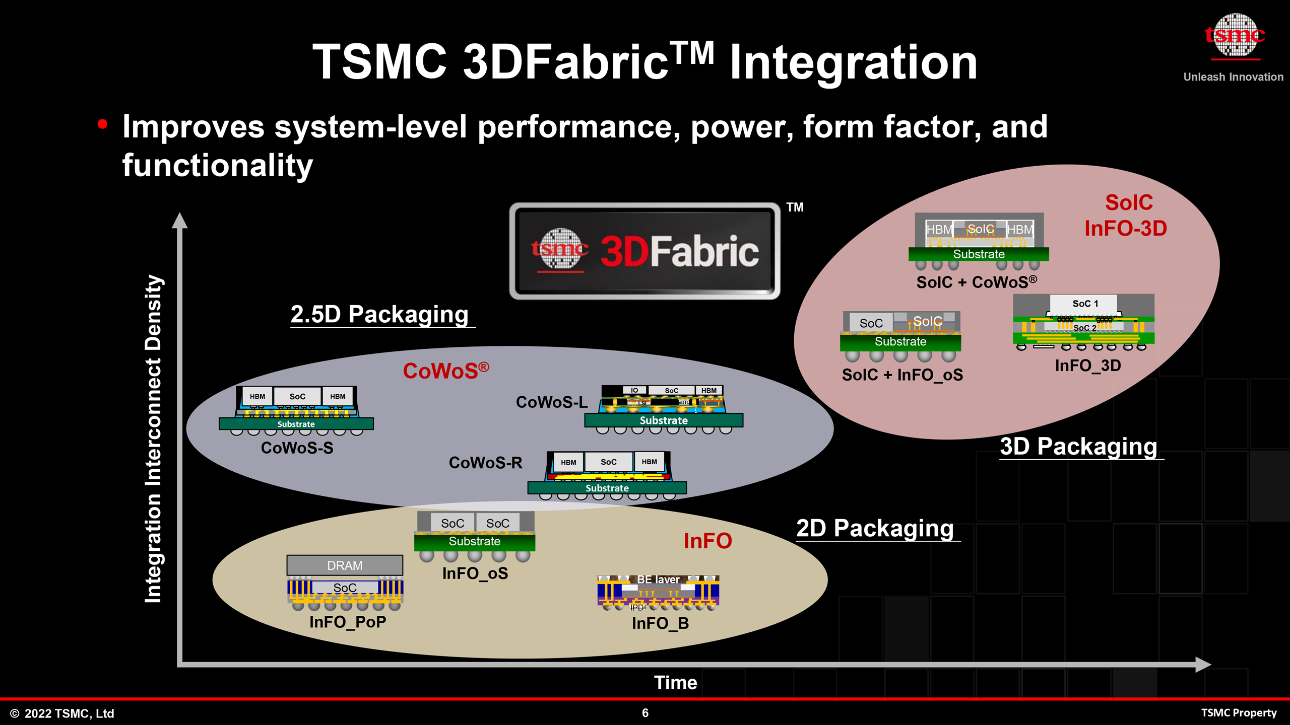
As part of their efforts to press the limits on the biggest manufacturable chip sizes, Taiwan Semiconductor Production Co. is dealing with its brand-new Chip-On-Wafer-On-Substrate-L (CoWoS-L) product packaging innovation that will enable it to develop bigger Super Provider interposers. Focused on the 2025 time period, the next generation of TSMC’s CoWoS innovation will permit interposers rising to 6 times TSMC’s optimum reticle size, up from 3.3 x for their present interposers. Such powerful system-in-packages (SiP) are planned for usage by performance-hungry information center and HPC chips, a specific niche market that has actually shown going to pay considerable premiums to be able to put numerous high efficiency chiplets on a single plan.
” We are presently establishing a 6x reticle size CoWoS-L innovation with Super Provider interposer innovation,” stated stated Yujun Li, TSMC’s director of service advancement who supervises of the foundry’s High Efficiency Computing Service Department, at the business’s European Innovation Seminar 2023.
International megatrends like expert system (AI) and high-performance computing (HPC) have actually developed need for relatively unlimited quantities of calculate horse power, which is why business like AMD, Intel, and NVIDIA are developing exceptionally complicated processors to deal with those AI and HPC applications. Among the methods to increase calculate abilities of processors is to increase their transistor count; and to do so effectively nowadays, business utilize multi-tile chiplet styles. Intel’s remarkable, 47 tile Ponte Vecchio GPU is a fine example of such styles; however TSMC’s CoWoS-L product packaging innovation will allow the foundry to develop Super Provider interposers for much more colossal processors.
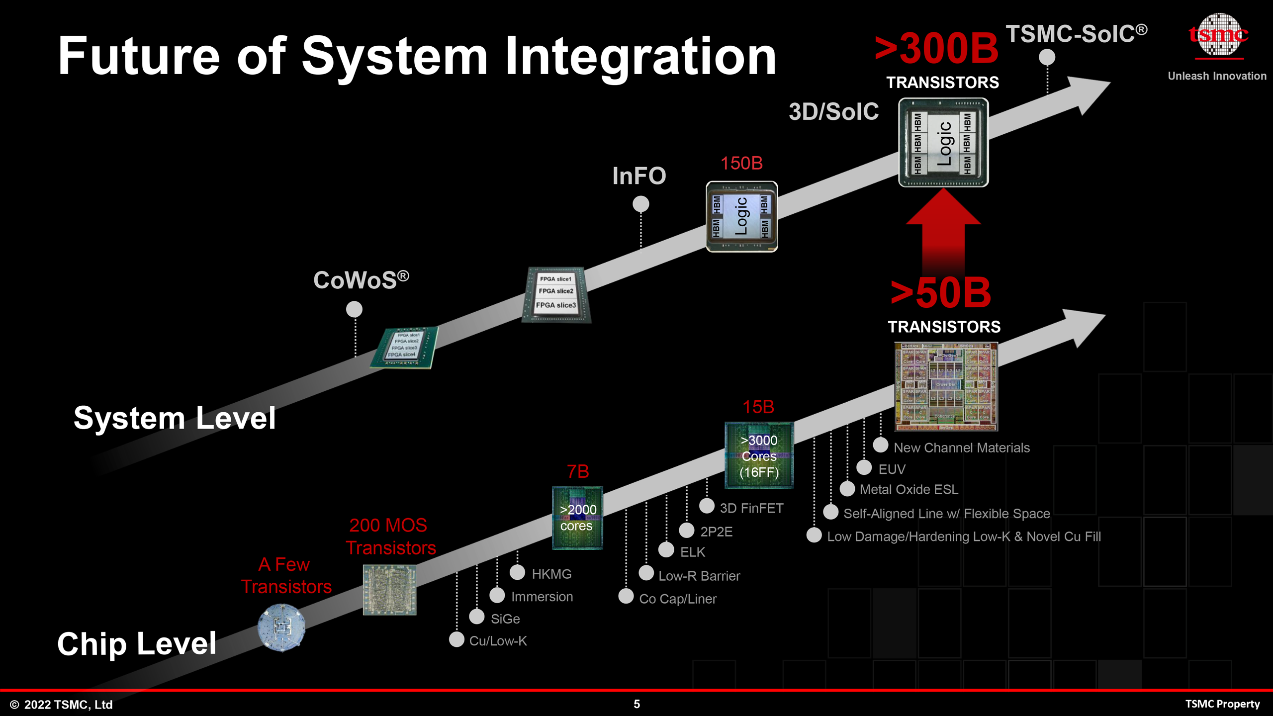
The theoretical EUV reticle limitation is 858mm 2 ( 26 mm by 33 mm), so 6 of these masks would allow SiPs of 5148 mm 2 Such a big interposer would not just pay for space for numerous big calculate chiplets, however it likewise leaves a lot of space for things like 12 stacks of HBM3 (or HBM4) memory, which indicates a 12288-bit memory user interface with bandwidth reaching as high as 9.8 TB/s.
” The Super Provider interposer includes numerous RDL layers on the front in addition to on the behind of the interposer for yield and manufacturability,” described Li. “We can likewise incorporate different passive parts in the interpreter for efficiency. This 6 reticle-size CoWoS-L will be certified in 2025”
Structure 5148 mm 2 SiPs is an exceptionally difficult jobs and we can just question just how much they will cost and just how much their designers will charge for them. At present NVIDIA’s H100 accelerator, whose product packaging covers an interposer numerous reticles in size, expenses around $ 30,000 So a substantial bigger and more effective chip would likely press costs higher still.
However spending for the expense of big processors will not be the only big financial investments that information center operators will require to make. The quantity of active silicon that 5148 mm 2 SiPs can house will probably lead to a few of the most power-hungry HPC chips produced yet — chips that will likewise require similarly effective liquid cooling to match. To that end, TSMC has actually divulged that it has actually been checking on-chip liquid cooling innovation, mentioning that it has actually handled to cool off silicon plans with power levels as high as 2.6 kW. So TSMC does have some concepts in mind to deal with the cooling requirement of these severe chips, if just at the rate of incorporating much more advanced innovation.